High-Resolution and Frame Speed with CMOS Image Sensors: A Technical Overview
The combination of high resolution and frame speed using CMOS image sensors has become highly attractive, serving as a major driving factor for transitioning from CCD (Charge-Coupled Device) to CMOS technology in industrial cameras. However, this shift requires careful consideration of the various defects inherent to CMOS sensors and whether camera manufacturers address them effectively.
Our investigation into this technology aimed to replicate the image quality once associated with CCDs as closely as possible using CMOS sensors. While some well-known defects are relatively straightforward to correct, others present greater challenges—such as temperature-dependent issues.
Known Defects in CMOS Sensors
The most commonly recognized defects include:
- Pixel defects: Such as single-point defects, clustered defects, row defects, and column defects.
- DSNU (Dark Signal Non Uniformity): Variations in dark signal across the sensor array.
- PRNU (Pixel Response Non Uniformity): Differences in pixel response to light intensity.
Less Common Defects
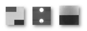
Defects that are less understood but still impactful include column noise, line noise, and black level shift (as illustrated below). These issues are more difficult to correct because they depend on the content of the captured image.
Column Noise | Line Noise | Black Level Shift
Proactive Correction: The Camera-Based Approach
Defect pixel correction and flat-field correction are examples of techniques best implemented directly within the camera hardware. Eliminating problems at the source is universally advantageous, as it minimizes noise and other complications in subsequent processing stages. In this context, performing corrections within the camera offers several benefits:
- Sensor Expertise: The camera manufacturer has detailed knowledge of the sensor’s characteristics.
- Enhanced Data Availability: More bits are available for processing directly at the source.
- Access to Additional Information: Features like temperature monitoring can be incorporated into the correction process.
- Reduced System Costs: It saves processing power and lowers overall system costs (development + BOM).
For example, new pixel defects may develop over time—making it advantageous if updated defect maps can be uploaded to the camera. Similarly, DSNU is influenced by temperature and gain, requiring periodic recalibration for accurate results.
Metrology Applications
High-end applications, particularly in metrology (precision measurement), demand these advanced correction techniques to achieve the necessary accuracy and precision.
Last Updated: 2025-09-04 19:13:16