Silicon wafer inspection using infrared imaging to detect internal defects and cracks during semiconductor manufacturing process
Silicon Wafer Inspection Using Infrared Imaging: Ensuring Quality in Semiconductor Manufacturing
Integrated circuits, the backbone of nearly all electronic devices, rely heavily on silicon wafers as a key component. These semiconductor materials offer unique properties that make them essential for modern electronics. One significant advantage is their transparency to infrared light—a property leveraged by manufacturers to detect defects during production. Radiant Optronics utilizes Allied Vision’s SWIR cameras (Goldeye G-008) in its Infrared Imaging Microscopes, enabling detailed inspection of silicon wafers and identifying potential cracks or flaws that could compromise end-products.
Silicon Cracks: A Threat to Product Quality
The manufacturing process for silicon wafers involves several stages including growth, sawing, grinding, etching, and polishing. These steps can introduce residual stress into the wafer material, potentially leading to cracks at any point in production or even during cutting into individual integrated circuits (ICs). If left undetected, these flaws could render surviving wafers unusable later on. Preventive measures include inspecting raw materials for impurities and monitoring defects throughout processing to control costs effectively.
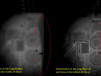
Seeing Through Silicon with Infrared Light
Infrared imaging offers a powerful solution by allowing operators to look beyond the surface of semiconductor substrates. The transparency of silicon to infrared wavelengths makes it possible to use cameras like those based on Indium Gallium Arsenide (InGaAs) sensors, which operate in the short-wave infrared band between 900 nm and 1700 nm. This capability provides high-contrast images highlighting imperfections such as cracks—an essential tool for maintaining quality standards while reducing expenses.
Meeting Growing Demand with Advanced Imaging
The surge in demand for electronic devices requires semiconductor fabrication plants to produce larger quantities of wafers and ICs quickly and efficiently. Infrared imaging technology plays a pivotal role here, offering advanced solutions for quality assurance without slowing down production lines—an approach that keeps manufacturing costs manageable amid rising market pressures.
Radiant Optronics: Innovating Semiconductor Inspection
Headquartered in Singapore, Radiant Optronics specializes in applying cutting-edge technologies to semiconductor failure analysis across wafer fabrication plants and packaging services. Their Infrared Imaging Microscopes incorporate Allied Vision’s Goldeye G-008 SWIR cameras—high-performance devices designed for industrial use with exceptional resolution capabilities.
Technical Specifications of the Goldeye G-008
This model stands out as one of the fastest 1/4-VGA resolution GigE Vision cameras available in the short-wave infrared spectrum. Capable of reaching up to 344 frames per second (fps) at full resolution, it supports diverse industrial applications requiring rapid defect detection mechanisms or real-time monitoring systems enhancements.
Customer Endorsement
“The Goldeye G-008 offers a favorable price-performance combination for its intended application scope,” explains Christopher Cheong from Radiant Optronics. “Its performance aligns perfectly with what we need while being accessible economically—a testament to Allied Vision’s commitment toward providing robust imaging solutions within reach.”
Reliability Features
Beyond speed, the camera boasts reliability through active thermo-electric cooling (TEC1) ensuring low-noise images under varying environmental conditions. Its compact design without fans simplifies installation and integration into existing systems while maintaining thermal stability.
Key Advantages of Goldeye G-008
- Superior defect detection capabilities
- Cost-effective solution for quality control
- High frame rates support faster manufacturing throughput
Last Updated: 2025-09-04 16:45:47